
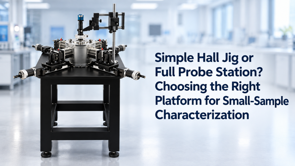
When researchers specify a Hall effect measurement system, one hardware decision is often underestimated:
Do you actually need a full probe station, or would a simpler Hall sample jig do the job better?
For conventional semiconductor wafers, thin films, bulk materials, and pre-contacted samples, a fixed Hall jig can be simple, stable, and cost-effective.
For microfabricated devices, very small Hall bars, two-dimensional materials, or samples with microscopic contact pads, however, a probe station may become essential.
The mistake is assuming that a probe station is automatically the “higher-end” choice.
It is not.
The correct platform depends on sample size, contact geometry, measurement workflow, environmental requirements, and how frequently electrical contacts must be repositioned.
For Hall effect measurement and small-sample characterization, matching the sample interface to the real experiment is often more important than adding more hardware.
1. Start With the Sample, Not the Instrument
Many Hall system discussions begin with specifications such as:
- Maximum magnetic field
- Current range
- Voltage resolution
- Resistance range
- Temperature range
- Measurement accuracy
These specifications matter.
But before selecting the measurement electronics, laboratories should answer a more basic question:
How will the electrical measurement system physically connect to the sample?
For a 10 × 10 mm semiconductor sample with four prepared contacts, the answer may be straightforward.
For a micron-scale Hall bar patterned on a chip, it may not be.
The Sample Interface Determines the Platform
The key questions include:
- What is the physical sample size?
- How large are the electrical contact pads?
- Are contacts already fabricated?
- Are wires permanently bonded to the sample?
- Must probes be repositioned between devices?
- Is optical alignment required?
- Will measurements be made at room temperature only?
- Is vacuum or controlled atmosphere required?
- Will temperature-dependent measurements be performed?
- How fragile is the sample surface?
These questions often determine whether a Hall jig or probe station is appropriate before magnetic field or instrument specifications are even discussed.
2. What Is a Simple Hall Jig?
A Hall jig is essentially a dedicated sample holder designed to provide repeatable electrical connections while positioning the sample within the magnetic field.
Depending on the design, samples may connect through:
- Pre-attached wires
- Wire bonding
- Spring contacts
- Conductive clips
- Plug-in sample cards
- Fixed electrical terminals
The sample is mounted in a defined position, connected to the measurement circuit, and placed in the magnetic field.
Advantages of a Hall Jig
A well-designed Hall jig can provide:
- Simple operation
- Fast sample changeover
- Stable mechanical positioning
- Fewer moving components
- Compact dimensions inside the magnet gap
- Lower system complexity
- Lower purchase cost
- Good repeatability for standardized samples
For routine Van der Pauw or Hall bar measurements on prepared samples, this approach can be entirely sufficient.
Where Hall Jigs Work Best
A simple jig is particularly attractive when:
- Sample dimensions are relatively consistent
- Contacts are already prepared
- Contact pads are large enough for straightforward connection
- Multiple samples use similar geometry
- Frequent microscopic repositioning is unnecessary
- Measurements are primarily routine Hall and resistivity tests
In these cases, adding a complete probe station may increase complexity without improving the actual measurement.
3. What Does a Full Probe Station Add?
A probe station changes the sample interface from a relatively fixed connection platform to a flexible positioning system.
A typical configuration may include:
- XYZ micro-positioning stages
- Probe arms
- Fine probe tips
- Microscope or camera
- Illuminated sample stage
- Adjustable sample chuck
- Precision electrical cabling
- Shielding or enclosure
- Optional vacuum or environmental control
Instead of permanently wiring each sample, an operator can visually locate contact pads and position individual probes onto them.
The Main Advantage Is Not Higher Measurement Accuracy
This distinction is important.
A probe station does not automatically make a Hall measurement more accurate.
Its primary advantage is accessibility and positioning flexibility.
It becomes valuable when the experiment requires reliable electrical access to small, closely spaced, or frequently changing contact locations.
4. Why Small Samples Change the Decision
Hall effect measurements are sensitive to sample geometry and contact configuration.
NIST’s Hall measurement guidance notes that, for Van der Pauw measurements, contacts should be small relative to the distance between them. It also identifies nonsymmetric contact placement and sample shape as important sources of offset voltage. NIST
This becomes increasingly important as samples become smaller.
Imagine Two Samples
Sample A
- 10 × 10 mm semiconductor plate
- Four large prepared contacts
- Repeatable Van der Pauw geometry
Sample B
- 3 × 3 mm chip
- Multiple microfabricated devices
- Contact pads only tens or hundreds of micrometers across
- Several Hall bars on the same chip
Sample A may work perfectly with a dedicated Hall fixture.
Sample B introduces an entirely different mechanical problem.
The measurement electronics may be identical, but the sample interface probably should not be.
5. Two-Dimensional Materials Make Contact Strategy Even More Important
Graphene, MoS₂, WSe₂, and other two-dimensional materials make the choice even more critical.
For these materials, the electrical contacts themselves can significantly affect the measured device behavior.
A major review in Nature Materials emphasizes that electrical contacts are a critical component of devices based on two-dimensional semiconductors and discusses how interface and contact resistance influence electrical transport. Nature
That means a small-sample Hall platform should not be chosen simply because the instrument can measure very low voltage.
The laboratory also needs to consider:
- Contact quality
- Probe positioning
- Probe pressure
- Pad dimensions
- Device geometry
- Contact resistance
- Sample damage risk
- Reproducibility between measurements
For delicate 2D-material devices, the physical interface between the probe and device can become part of the measurement problem.
6. When a Simple Hall Jig Is Usually the Better Choice
A full probe station can look impressive in a system quotation.
But many laboratories simply do not need one.
Choose a Hall Jig When
- Samples already have four reliable electrical contacts
- Wires can be bonded or permanently attached
- Sample geometry is standardized
- Samples are large enough for easy handling
- Room-temperature Hall measurement is the main task
- High sample throughput matters
- Operators do not need to reposition contacts repeatedly
- Budget should be concentrated on measurement electronics or magnetic field capability
This configuration is especially practical for:
- Semiconductor thin films
- Thermoelectric materials
- Oxide materials
- Bulk semiconductor samples
- Routine Van der Pauw measurements
- Teaching and standard research laboratories
Simplicity Can Improve Repeatability
A fixed fixture eliminates several variables:
- Probe position
- Probe pressure
- Operator positioning
- Accidental movement
When samples can be standardized, fewer degrees of mechanical freedom can actually make the measurement workflow more repeatable.
7. When You Should Seriously Consider a Probe Station
A probe station becomes much easier to justify when the sample itself requires microscopic access.
Choose a Probe Station When
- Contact pads are very small
- Samples contain multiple devices
- Electrical contacts must frequently be repositioned
- Optical identification of pads is required
- Samples cannot easily be permanently wired
- Different device structures are measured on the same substrate
- I-V characterization is required before or after Hall testing
- Researchers need flexible research rather than standardized routine measurements
Typical applications include:
- 2D materials
- Microfabricated Hall bars
- MEMS structures
- Semiconductor devices
- Microelectronic structures
- Small patterned thin-film devices
Here, the probe station solves a genuine experimental problem.
8. Do Not Use Sample Size Alone to Make the Decision
This is one of the most important points.
Small sample does not automatically mean probe station.
A very small chip with wire-bonded contacts can potentially be mounted on a compact carrier and measured very effectively using a fixed holder.
Conversely, a physically larger wafer containing many small devices may require a probe station because individual contact pads must be accessed repeatedly.
The better decision criterion is therefore:
How difficult is it to create repeatable electrical contact with the measurement area?
Not simply:
How many millimeters wide is the sample?
9. Hall Jig vs Probe Station: Practical Comparison
| Requirement | Simple Hall Jig | Full Probe Station |
|---|---|---|
| Pre-contacted samples | Excellent | Usually unnecessary |
| Standard sample geometry | Excellent | Good |
| Microscopic contact pads | Limited | Excellent |
| Rapid routine testing | Excellent | Moderate |
| Multiple devices on one chip | Limited | Excellent |
| Optical alignment | Usually limited | Excellent |
| Flexible contact positioning | Limited | Excellent |
| Operator training requirement | Lower | Higher |
| Mechanical complexity | Lower | Higher |
| System cost | Lower | Higher |
| Research flexibility | Moderate | High |
| Small magnet-gap integration | Easier | Requires more planning |
The table should be treated as a platform-selection guide rather than a universal ranking.
10. There Is Also a Middle Ground
The decision does not always have to be:
Basic holder OR large semiconductor probe station.
For many research laboratories, an intermediate configuration is better.
A Micro-Probe Hall Platform
A compact Hall measurement system can combine:
- Small XYZ positioning stages
- Four microprobes
- Microscope or HD camera
- Compact sample stage
- Electromagnet
- Precision source and measurement electronics
- Automated switching
- Hall measurement software
This provides much of the positioning flexibility required for small samples without introducing the footprint and complexity of a large wafer probe station.
Cryomagtech currently offers Hall configurations that integrate micro-motion positioning, multiple probe assemblies, microscopy, electromagnet control, measurement electronics, and automated software for semiconductor characterization. Cryomagtech
For many university research groups, this intermediate architecture can be more practical than either extreme.
11. Magnetic Field Integration Changes Probe Station Design
A normal semiconductor probe station and a Hall measurement probe station are not necessarily the same thing.
Hall characterization requires the sample to operate inside a controlled magnetic field.
That introduces additional mechanical constraints.
Important Integration Questions
The system designer must consider:
- Available magnet pole gap
- Sample height relative to the magnetic field center
- Probe-arm clearance
- Microscope working distance
- Field orientation
- Electrical cable routing
- Mechanical stability
- Nonmagnetic components near the measurement region
A large probe station cannot simply be placed between the poles of every electromagnet.
The magnet and sample platform need to be designed together.
This is one reason why defining the sample and probing method early in a project is so important.
12. Temperature Control Makes the Choice More Complex
Room-temperature Hall measurement is mechanically straightforward compared with variable-temperature characterization.
If the experiment requires:
- Cryogenic Hall measurement
- Elevated-temperature measurements
- Vacuum
- Controlled atmosphere
- Long temperature sweeps
then an open probe station may no longer be the most practical interface.
A sample holder or probe card integrated into a cryostat may provide better:
- Thermal anchoring
- Environmental control
- Mechanical stability
- Wiring management
Cryomagtech’s electrical transport platforms can also be configured with electromagnets or superconducting magnets, automated Hall measurement, plug-in sample cards, and optional variable-temperature environments depending on the application. Cryomagtech
The correct question therefore becomes:
Where and under what environment must the electrical contacts operate?
13. Probe Stations Also Introduce New Sources of Error
More positioning flexibility creates more variables.
Potential issues include:
- Probe slipping
- Inconsistent probe pressure
- Pad scratching
- Contact resistance changes
- Probe oxidation or contamination
- Sample movement
- Accidental shorting between pads
For extremely small or fragile structures, mechanical probing can itself affect measurement repeatability.
For two-dimensional semiconductor devices in particular, contact interfaces are a major part of overall electrical performance, as highlighted in the contact-engineering literature. Nature
Therefore, purchasing a probe station should not be viewed as eliminating contact problems.
It gives the researcher more control over contacts—but also more responsibility for controlling them correctly.
14. Ask These Questions Before Requesting a Hall System Quotation
Instead of initially asking a supplier:
“Can your Hall system measure my sample?”
provide the information needed to determine the correct platform.
Sample Information
- Sample material
- Sample dimensions
- Sample thickness
- Hall bar or Van der Pauw geometry
- Number of devices per substrate
Contact Information
- Number of electrical contacts
- Contact-pad dimensions
- Distance between contacts
- Whether contacts are already fabricated
- Whether wires can be bonded
- Whether repeated probe positioning is necessary
Measurement Requirements
- Hall effect
- Resistivity
- Magnetoresistance
- I-V characterization
- R-T measurements
- R-H measurements
Environmental Requirements
- Room temperature
- Low temperature
- High temperature
- Vacuum
- Controlled atmosphere
Workflow Requirements
- Samples per day
- Manual or automated measurement
- Multiple samples per batch
- Need for visual positioning
- Frequency of sample changes
These details allow the system architecture to be chosen from the experiment backward.
15. How Cryomagtech Approaches Small-Sample Hall Characterization
Cryomagtech Hall Effect Measurement Systems can be configured around different sample interfaces rather than forcing every application into the same hardware architecture.
Depending on the experiment, the platform can be designed around:
- Standard Hall sample holders
- Plug-in sample cards
- Micro-probe positioning
- Microscope-assisted contact placement
- Automated matrix switching
- Electromagnet field control
- Hall, resistivity, R-H, R-T, and I-V measurements
- Variable-temperature environments
The objective is to match the Hall measurement platform to the sample geometry, contact method, magnetic field, temperature environment, and research workflow.
A more complex system is only better when the experiment actually requires that complexity.
16. Key Takeaways
- A full probe station is not automatically better than a simple Hall jig.
- Pre-contacted, standardized samples can often be measured more efficiently with a fixed Hall fixture.
- Microfabricated devices and small contact pads may require microscope-assisted microprobe positioning.
- Sample dimensions alone should not determine the platform; contact accessibility is often more important.
- Hall measurements are sensitive to contact geometry and symmetry, especially for small samples. NIST
- Electrical contacts are particularly important in 2D semiconductor devices. Nature
- Variable-temperature or vacuum measurements may favor an integrated sample holder or cryostat configuration rather than an open probe station.
- Magnet geometry, probe clearance, and sample positioning must be considered as one integrated system.
- An intermediate micro-probe Hall platform can often provide the best balance between simplicity and research flexibility.
The purchasing question should therefore not be:
“What is the most advanced Hall platform we can afford?”
It should be:
“What is the simplest platform that can make reliable, repeatable contact with every sample we actually need to measure?”
That question usually leads to a better system design—and avoids paying for complexity that the laboratory may never use.
References
NIST – Resistivity and Hall Measurements
NIST provides detailed guidance on Van der Pauw and Hall measurements, including sample geometry, contact dimensions, ohmic contacts, current reversal, magnetic-field reversal, and common sources of Hall measurement error. NIST
NIST – Resistivity and Hall Measurements
Nature Materials – Electrical Contacts to Two-Dimensional Semiconductors
This review discusses the importance and physics of electrical contacts in graphene, transition-metal dichalcogenides, and other two-dimensional semiconductor devices, making it highly relevant to small-device probing and electrical transport characterization. Nature
Nature Materials – Electrical Contacts to Two-Dimensional Semiconductors